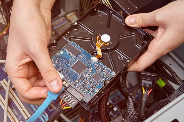
IBM had collaborated with GlobalFoundries and Samsung to create the world’s first 5-nanometer silicon chip. Not only is it significantly smaller than previous versions, but it’s also way more dense and powerful, hence it can perform better. It’s also the first practical application of extreme ultraviolet (EUV) lithography and horizontal gate-all-around (GAA) field effect transistors (FETs).
Source: YouTube, IBM Research
In a battle to create chips that can work just as efficient as previous ones but smaller, these GAAFET chips, when combined with EUV technology, could create working silicon chips as small as 3nm. In comparison, the traditional Tri-gate finFETs, which are what’s currently used for chips smaller than 22nm, can only go down to 7nm before they stop working. These FinFETs had originally solved all the problems that 2D transistors faced, as they are 3D. In effect, the volume of silicon atoms which can carry electricity by protruding from the substrate had increased. However, with GAAFETs, we can revert back to the old and handy 2D transistor technology using stackable silicon nanowires, and they’ll work even better.
“The new 5nm tech offers a 40 percent performance boost at the same power, or a 75 percent drop in power consumption at the same performance,” says IBM. The density of the material has also improved, being able to fit around 30 billion transistors onto a single 50 square millimeters across, which is the size of a fingernail. In contrast, old chips of the same size can only hold 20 billion transistors at most.

Source: Ars Technica
“This announcement is the latest example of the world-class research that continues to emerge from our groundbreaking public-private partnership in New York,” says Gary Patton, CTO and Head of Worldwide R&D at GlobalFoundries. “As we make progress toward commercializing 7nm in 2018 at our Fab 8 manufacturing facility, we are actively pursuing next-generation technologies at 5nm and beyond to maintain technology leadership and enable our customers to produce a smaller, faster, and more cost efficient generation of semiconductors.”
This new tiny chip is great news, because it fits the current trend of technology getting smaller yet having more things into it. Not only will computers, smartphones, and other devices get smaller and more portable, they’ll also get more powerful. IBM is leading the way for this movement, even pointing out that they can possibly make GAAFETs even smaller.
Article Sources:


